Hello.
I am Altera F. Hanako, providing technical support for Altera® FPGA products at Macnica.
Did you know that when debugging Altera® FPGAs on actual hardware, there are debugging methods other than oscilloscopes or logic analyzers?
That is Signal Tap!!
※ SignalTap II was renamed to Signal Tap starting from Quartus Prime 17.1.
Configuration and block diagram of the Signal Tap logic analyzer
The official name is Signal Tap Logic Analyzer.
Simply put, it is a logic analyzer function in Quartus® Prime that monitors internal signals of the user circuit implemented in the FPGA.
Its features are:
・Implement Signal Tap IP in the available logic elements (LE) and memory within the FPGA
・Display observation data on the Quartus® Prime screen
・Use a programming download cable such as the Altera® FPGA Download Cable II as the communication method between the board and Quartus® Prime
・Use the FPGA's JTAG pins as monitor pins for observation signals
・No need to secure user I/O pins for debugging!
・No external devices like logic analyzers or oscilloscopes required!
・Free to use!
Let's Prepare
To run the Signal Tap Logic Analyzer on an FPGA, you need the following.
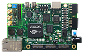
Board with FPGA Installed |
Supported Devices Altera® Agilex™ Series / Stratix® Series / Arria® Series / Cyclone® Series / MAX® 10
|
Development Software |
Quartus® Prime Pro Edition / Quartus® Standard Edition / Quartus® Lite Edition
|
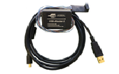
Download Cable |
Altera® FPGA Download Cable II (formerly USB-Blaster™ II)
|

What Work Will Be Done
The process consists of only 4 steps!
Step 1 |
Step 2 |
Step 3 |
Step 4 |
Create Signal Tap IP |
Implement Signal Tap IP into user design & run compilation |
Download .sof to FPGA |
Acquire and observe sampling data |
Please note that the user design for Signal Tap must have logic synthesis and placement & routing completed beforehand.
1. Create Signal Tap IP
Create a new STP file. By setting conditions on this sheet, you can create the IP.
・Specify the Sampling Clock
In the Signal Configuration window, select the clock from the user circuit that Signal Tap will operate with.
Signal Tap samples the monitor signals on the rising edge.
As with a typical logic analyzer, the observation accuracy of the monitor signals depends on the frequency of the sampling clock.
It is also possible to supply a clock externally to the FPGA.
For how to use the Node Finder, please refer to the following document (search using the keyword “Node Finder”).
・Quartus® Prime - How to Set Constraints (Assignment Editor)
・Select Monitor Signals
Select the signals to observe using the Node Finder. The selected signals can also be used for trigger conditions. However, signals specified as the sampling clock cannot be monitored.
Hanako's Quick Tip♪
When registering internal signals to observe in the STP file, there is a method that does not use the Node Finder.
That is by using the Technology Map Viewer!
You can visually select signals and quickly register them. This is my recommended method.
For details, please see this article.
・How to Easily Register Internal Signals You Want to Capture with Signal Tap into an STP File
・Set Trigger Conditions
Select the condition for the signals you want to use as trigger conditions.
2. Implement Signal Tap IP into User Design & Run Compilation
On the STP file, from the File menu Save As, give the STP file a name and save it.
You will see a message: “Do you want to enable Signal Tap File ‘filename.stp’ for the current project?” Select Yes to register it in the project. (The figure below shows how to confirm.)
Now the Signal Tap implementation is complete!! There is no need for any connection work in code.
After that, click the icon on the STP file to compile the user design including the Signal Tap IP.
3. Download .sof to FPGA
In the JTAG Chain Configuration window (top right in the STP file), select the download cable and confirm the .sof file to transfer. Then click the Program Device button to start the download!
4. Acquire and Observe Sampling Data
Click the Run Analysis button to display the latest sampling data in the STP file that hits the trigger event.
If you only want to change the trigger condition's High or Low, recompilation is not necessary.
Just change the value and immediately click the Run Analysis button.
See? It's easy♪
If you only want to observe a few internal FPGA signals, you can debug easily with Signal Tap without pulling out large equipment like logic analyzers.
Hanako's Quick Tip♪
Recompilation after implementing Signal Tap IP can increase compilation time and affect layout, which are considered drawbacks; however, by using Quartus® Prime's incremental compilation feature, users can reduce this stress. (Lite Edition does not support incremental compilation, so it cannot be used together.)
Also, during debugging, if you make changes that affect the Signal Tap IP circuit configuration such as adding/removing Signal Tap instances, adding/removing signals for sampling or trigger conditions, or changing the sampling clock, recompilation is required again.
For details, please see the following documents.
Design Debugging with the Signal Tap Logic Analyzer (Quartus® Prime Standard Edition)
Design Debugging with the Signal Tap Logic Analyzer (Quartus® Prime Pro Edition)
In Conclusion
This time, we introduced the Signal Tap Logic Analyzer.
If you are eager to try the Signal Tap Logic Analyzer function quickly!
Use the following tutorials, sample designs, supported evaluation kits, and development kits to easily experience the workflow from creating Signal Tap IP to performing on-hardware debugging. Please make use of them.
・ Tutorial: Documentation
quartus_signaltap_tutorial_v1710_r1__1.pdf
・ Tutorial: Sample Design for Cyclone® 10 LP FPGA Evaluation Kit
・ Tutorial: Sample Design for MAX® 10 FPGA Evaluation Kit
・ Tutorial: Design-only Project
To use SignalTap® II (now Signal Tap) in Quartus® Prime Lite Edition version 16.0 or earlier, a "magic trick" is needed.
This magic trick is to "enable the TalkBack feature"!
Please follow the steps below to enable the TalkBack feature.
1. Select Tools menu ⇒ Options
2. In the Options window, select Internet Connectivity from the Category list
3. In the Internet Connectivity dialog window, click the TalkBack Options button
4. In the TalkBack Options window, check the option Enable sending TalkBack data to Altera (turn On)
That's all!
[Related FAQ] What is the TalkBack feature?
Recommended Articles/Materials
Quartus® Beginner's Guide - How to Use the Signal Tap Logic Analyzer