1. Overview
There are various ways to boot the Nios® V, as well as the Nios® II.
This article focuses on devices with a Secure Device Manager (SDM), such as Stratix® 10 FPGAs and Agilex™ 7 FPGAs, and shows how to boot the Nios® V processor code in the QSPI Flash ROM connected to the SDM.
A reference design for SDM Boot is available from Intel. You can build your environment based on this design.
Note:
SDM stands for Secure Device Manager. If you are interested in SDM features, please refer to the Agilex™ FPGA "Security" section - (In Japanese).
Note:
To use SDM boot, you must select Active Serial (AS-Fast or AS-Normal) as the FPGA configuration mode (MSEL setting). The Nios® V processor cannot perform SDM boot if it is configured in a mode other than Active Serial, such as Avalon-ST.
In addition to SDM boot, Nios® V supports the following boot methods. We have prepared articles for each of them, please refer to them for details.
- QSPI Boot via Generic Serial Interface (GSFI) (coming soon)
- Nios® V Boot Option ~ On-Chip RAM (XIP) ~ On-Chip Memory Boot - (In Japanese)
1-1. Overall Configuration
Figure 1 shows the overall configuration.
Figure 1. SDM Boot Overall Configuration
1-2. SDM Boot Flow
SDM boot is performed as follows.
- The Nios® V processor executes the SDM boot loader from on-chip memory.
- The SDM boot loader looks for software for the Nios® V processor stored in the configuration Flash ROM connected to the SDM.
- The SDM boot loader copies the software from the configuration Flash ROM to the On-Chip RAM or external RAM.
- After the copy is complete, the SDM boot loader jumps to the user application.
We will show you how to implement the software from the next chapter.
2. Hardware Implementation
This chapter shows how to implement the hardware. We will use Agilex™ 7 as an example.
The minimum IP requirements are as follows (for Quartus® Prime Pro Edition software version 22.4).
- Nios® V/m Processor Intel® FPGA IP
- On-Chip Memory (RAM or ROM ) Intel® FPGA IP (hereafter referred to as On-Chip RAM)
- Mailbox Client Intel® FPGA IP
Figure 2 shows how to build with Platform Designer.
Figure 2. Platform Designer Configuration
In this article, JTAG_UART IP is implemented for console output, but please note that it is not required.
The name of each implemented IP is set as follows for better visibility.
- Nios® V/m Processor Intel FPGA IP: cpu
- On-Chip Memory (RAM or ROM ) Intel® FPGA IP : bootcopier_rom, bootcopier_ram, user_application_mem
- Mailbox Client Intel® FPGA IP : mailbox
- JTAG UART Intel® FPGA IP: uart
The minimum required parameter settings for the above three IPs are described in the next section.
2-1. Nios® V/m Processor
Set Reset Agent to "bootcopier_rom.s1" from the Vectors item as shown in Figure 3 .
Figure 3. Nios® V/m Processor Vectors V/m Processor Parameter Settings
NOTES:
When selecting the Reset Agent : pull-down menu, the "bootcopier.s1" port may not appear. In this case, please select a different port and open the pull-down menu again to select it.
2-2. On-Chip Memory (RAM or ROM ) Intel® FPGA IP FPGA IP
This design uses three On-Chip RAMs. The following is a description of the settings for each.
As shown in Figure 4, Figure 5 and Figure 6 , set the Total Memory Size required for software execution and the Memory Initialization setting to specify the initial value file to be registered in the On-chip RAM.
First, we will explain the bootcopier_rom setting.
Figure 4. Example of bootcopier_rom parameter setting
On the Nios® II Processor, you could register by using memint.qip, but on the RiscFree IDE used on the Nios® V Processor, there is no command to generate meminit.qip, so you need to check "Enable non-default initialization file" as shown in Figure 4 and register the path of < any name >.hex.
In this article, it is set as follows.
- Type: ROM (Read-only)
- Total memory size: 6144 Bytes
- User created initialization file: bootcopier_rom.hex
The following is an example of bootcopier_ram settings.
Figure 5. Example of bootcopier_ram parameter settings
bootcopier_ram initializes RAM with default values. The size and other parameters are set as follows.
- Type: RAM (Writable)
- Total memory size: 6144 Bytes
Next is an example of user_application_mem setting.
Figure 6. Example of user_application_mem parameter setting
The default value of user_application_mem initializes RAM. The size and other parameters are set as follows.
- Type: RAM (Writable)
- Total memory size: 262144Bytes
2-3. Mailbox Client Intel® FPGA IP
The Mailbox Client Intel® FPGA IP is used as default.
Figure 7. Mailbox Client Intel® FPGA IP Parameter Settings
Quartus® Prime Settings Prime Settings
Open Assignments tab -> Device -> Device and Pin Options -> Configuration.
Configure the settings according to the board configuration.
- Configuration scheme: Active Serial x4 (can use Configuration Device)
- Active serial clock source: Set the clock frequency when configuring the FPGA.
Figure 8. Device and Pin Options for Quartus® Prime
3. Software Implementation
In SDM Boot, the SDM Boot Loader is used to load the User Application into work memory. This chapter describes how to generate the SDM Boot Loader and how to build the User Application.
This article assumes the directory configuration shown in Figure 9.
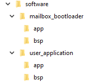
Figure 9. Directory Configuration
3-1 SDM Boot Loader
3-1-1. BSP Generation
Start the BSP Editor from Platform Designer and create Settings.bsp. If you do not know how to create it, please refer to the following link.
There are differences between the Nios® II Processor and the Nios® V/m Processor in how to start the BSP Editor, but the settings are the same: hal settings, hal.linker settings, hal.make settings, and Linker Script settings.
First, set hal, hal.kinker, and hal.make in the main tab, referring to Table 1 and Figures 10 to 12.
Table 1. BSP Editor Settings
| Settings | Settings |
| hal.max_file_descriptors | 4 |
| hal.log_port | Select None |
| hal.enable_exit hal.enable_clean_exit hal.c_plus_plus |
Uncheck |
| hal.sys_clk_timer hal.timerstamp_timer hal.stdin hal.stdout hal.stderr |
None |
| hal.linker |
Check and enable the following settings
allow_code_at_reset |
| hal.make.cflags_user_flags | -ffunction-sections -fdata-sections |
| hal.make.link_flags | -Wl,--gc-sections |
| hal.make.cflags_optimization | -Os |
Figure 10. hal settings
Figure 11. hal.linker settings
Figure 12. hal.make settings
Next, go to the BSP Software Package tab, and check the box for the altera_safeclib.
Figure 13. Software Packages settings
For Linker Script settings, select the BSP Linker Script tab and set the Section other than .entry to bootcopier_ram as shown in Figure 14 .
Figure 14. BSP Linker Script Settings
Click "Generate BSP" button to generate BSP.
3-1-2 Generating SDM Bootloader Application
This section describes how to generate the SDM Bootloader Application.
The SDM Bootloader Application is provided in the SDM Bootloader Example Design available from the Intel® FPGA Design Store. Download this design first.
Note:
The downloaded design is designed for the Stratix® 10 SX SoC L-Tile development kit, but the provided application can be used with other FPGAs that implement SDM, such as the Agilex™ 7 FPGAs.
After extracting the design, you will see the directory sw/mailbox_bootloader/app.
This is the SDM Bootloader project.
Copy the SDM bootloader ( mailbox_bootloader.c) in this directory to software/mailbox_bootloader/app, which will be generated this time.
Start Nios® V Command Shell and execute the following command to create CMakeLists.txt.
 niosv-app --app-dir=software/mailbox_bootloader/app\
 --bsp-dir=software/mailbox_bootloader/bsp\
 --srcs=software/mailbox_bootloader/ app/mailbox_bootloader.c
Next, build the application.
 cmake -G "Unix Makefiles" -DCMAKE_BUILD_TYPE=Release -B \
 software/mailbox_bootloader/app/release -S \
 software/mailbox_bootloader/app
make -C software/mailbox_bootloader/app/release
After build, SDM bootloder (.elf) will be generated in the following folder.
software/mailbox_bootloader/app/release
3-1-3. HEX File Generation and Memory Initialization
After the software build is completed and the ELF file is generated, generate the HEX file to be registered as the initial value of On Chip RAM.
Start the Nios® V Command shell and navigate to the project.
After moving to the project, enter the following command to generate the HEX file.
 elf2hex software/mailbox_bootloader/app/release/app.elf \
 -o bootcopier_rom.hex -b <base address of Bootloader ROM> \
 -w <data width of Bootloader ROM> -e <end address of Bootloader ROM> -r 4
The generated bootcopier_rom.hex is used as the initial value of bootcopier_rom.
Copy bootcopier_rom.hex to the location specified in Platform Designer before compiling the FPGA.
Note:
See below for information on how to update the HEX file to the SOF file without having to fully compile Quartus® Prime.
Reference:
Nios® II - Booting from On-Chip Memory - (In Japanese)
This completes the generation of the SDM Bootloder. In the next section, we will show you how to build the User Application.
3-2. User Application
3-2-1. Generating BSP
Start the BSP Editor from Platform Designer and create Settings.bsp. If you do not know how to create it, please refer to the following link.
After generation, configure the same settings as before.
To set hal.linker, go to Settings -> Advanced -> hal in the Main tab and check the hal.linker option as shown in Figure 6 .
- enable_at_load
- enable_alt_load_copy_exceptions
Figure 15. Configuration of hal.linker
For Linker Script settings, select the BSP Linker Script tab and set the Section other than .entry to "user_application_mem " as shown in Figure 16 .
Figure 16. BSP Linker Script Settings
3-2-2 Generating Application
Generate and build the Application project.
Please refer to the following article for the procedure up to the generation of the ELF file.
Reference: Ashling* Nios® V Project Development Procedure Using RiscFree* IDE 4-4. Starting RiscFree* IDE
3-2-3. Generating a HEX File
The generated application is written to QSPI using a technique called JTAG Indirect Configuration (JIC) programming.
In this section, we will generate the HEX file (.hex) necessary to generate the JIC file.
The ELF file generated earlier is converted to a HEX file using the following command.
 elf2flash --input software/user_application/app/debug/<user application >. elf \
--output flash . srec -epcs --offset 0x0 riscv32-unknown-elf-objcopy--input-target srec \
--output-target ihex flash . srec \
<user application >. hexGenerate programming files in the next section.
4. Generating the Programming File
Generate a JIC file using the generated HEX file.
Here is an example of generating a file to write only user_application.hex.
Please configure as follows and Generate.
- Start Address: Specify the value set in PAYLOAD_OFFSET in mailbox_bootcopier .c
- Input File: Specify user_application.hex
- Flash Loader: Specify the device to be used.
Figure 17. Generation of JIC file by Programing File Generator
For details on how to generate a JIC file, please refer to the following contents.
Reference material:
Nios® II Boot Option ~ EPCQ Flash ~ (using AS IF) <4-2. Generating JIC File> - (In Japanese)
Write the generated JIC file to QSPI to boot Nios® V from QSPI connected to SDM.
Recommended Pages
We have prepared a " Nios® II Summary Page - (In Japanese) " that summarizes various information on Nios® II.
Please refer to this page as well, as it contains a lot of useful information in addition to this article.